
- PV-Station-Solutions
- PV-Panel-Testing-Solutions
- Silicon-Ingot-Testing-Solutions
Perovskite/silicon (Pero/Si) tandem solar cells, as an emerging architecture to surpass the efficiency limits of single-junction cells, offer theoretical efficiencies exceeding 40% and demonstrate significant industrialization potential. However, existing research indicates that their long-term operational stability is far inferior to that of single-material cells, presenting a critical bottleneck for large-scale deployment. Performance degradation primarily originates from complex interfacial failures: under operational stresses such as light illumination and damp heat, the buried interface between the perovskite layer and the silicon substrate undergoes pronounced synergistic degradation.
This study identifies a strong correlation between interface stability and the microstructure of the interconnect layer, noting that porous structures like amorphous ITO accelerate interdiffusion of ions and hydrogen. Based on these findings, we propose strategies for interface engineering: developing dense transparent conductive oxides to enhance barrier properties, and introducing ultrathin atomic layer deposition barrier layers at critical interfaces to effectively inhibit ion and hydrogen migration, thereby providing a feasible technological pathway toward high-efficiency, long-lifetime Pero/Si tandem photovoltaic devices.
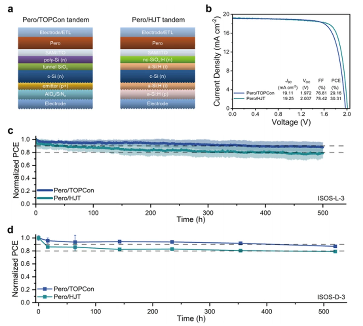
(a) Schematic of two promising monolithic perovskite/silicon tandem structures (b) J-V curves and extracted parameters (c) MPPT maximum power point tracking (d) Damp heat stability test
Two mainstream silicon cell technologies, TOPCon and HJT, were selected to construct monolithic tandem structures with p-i-n perovskite top cells. Self-assembled monolayers and ITO were introduced as interconnect layers at the perovskite/silicon interface. Measurement results show that the initial efficiency of HJT-based tandem devices was slightly higher than that of TOPCon-based counterparts, primarily attributed to the higher open-circuit voltage and fill factor enabled by their superior surface passivation capabilities.
Under standard ISOS-L-3 (light soaking) and ISOS-D-3 (damp heat) aging tests, both types of tandem devices exhibited significant performance degradation. The degradation rate of Pero/HJT devices was notably faster than that of Pero/TOPCon devices. Their T90 (time to maintain 90% of initial efficiency) under light soaking was only 86 hours, far lower than that of Pero/TOPCon devices (367 hours). This observation suggests that the amorphous silicon-based HJT structure may possess inherent weaknesses in interface stability.
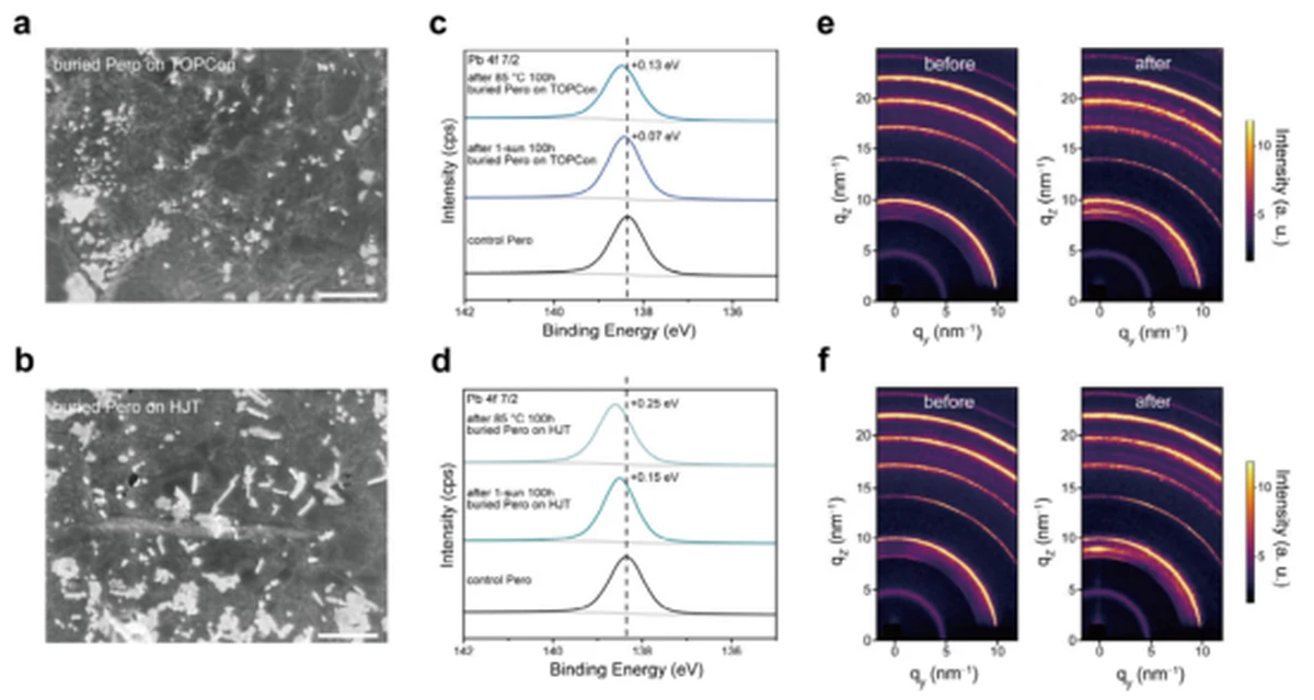
(a) SEM images of Pero/TOPCon and (b) Pero/HJT tandem devices (c) Pb 4f XPS spectra of control and buried perovskite in Pero/TOPCon and (d) Pero/HJT devices after thermal and light aging (e) 2D GIWAXS images of Pero/TOPCon and (f) Pero/HJT stacks before and after accelerated thermal aging
Scanning electron microscopy (SEM) and X-ray photoelectron spectroscopy (XPS) analysis revealed extensive lead iodide (PbI₂) precipitation at the buried perovskite interface after aging, with more severe decomposition observed in HJT samples. In-situ grazing-incidence wide-angle X-ray scattering (GIWAXS) further revealed that the transformation of perovskite to PbI₂ under thermal stress occurred earlier and faster on HJT, indicating that the amorphous interface structure accelerates ion migration and deprotonation processes in the perovskite.
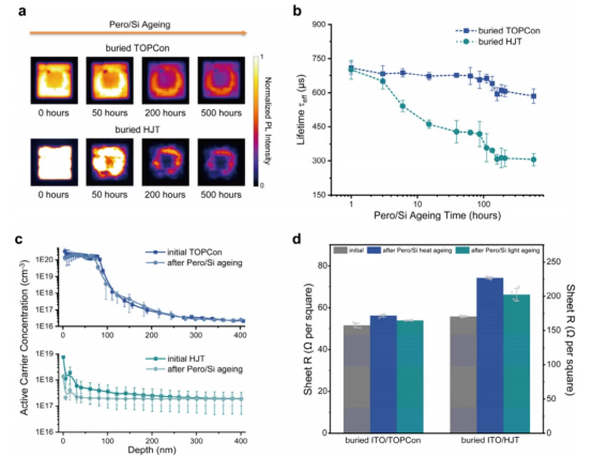
(a) PL mapping tracking of buried silicon cells during thermal aging of Pero/Si tandems (b) Effective carrier lifetime tracking of buried silicon cells during thermal aging using quasi-steady-state photoconductance (c) Depth profiles of active carrier concentration in buried silicon before and after thermal aging measured by electrochemical capacitance-voltage (d) Sheet resistance of buried ITO/silicon stacks before and after Pero/Si aging measured by four-point probe
Photoluminescence (PL) imaging and quasi-steady-state photoconductance measurements showed a significant decrease in carrier lifetime of the buried silicon cells during aging, with a greater magnitude of decay in the HJT structure. Electrochemical capacitance-voltage analysis revealed a decrease in active carrier concentration in the near-surface region of the silicon, accompanied by an increase in sheet resistance. These changes are attributed to interactions between ions migrated from the perovskite layer (such as I⁻ and organic cations) and hydrogen in the silicon, leading to increased surface defects and deactivation of dopants.
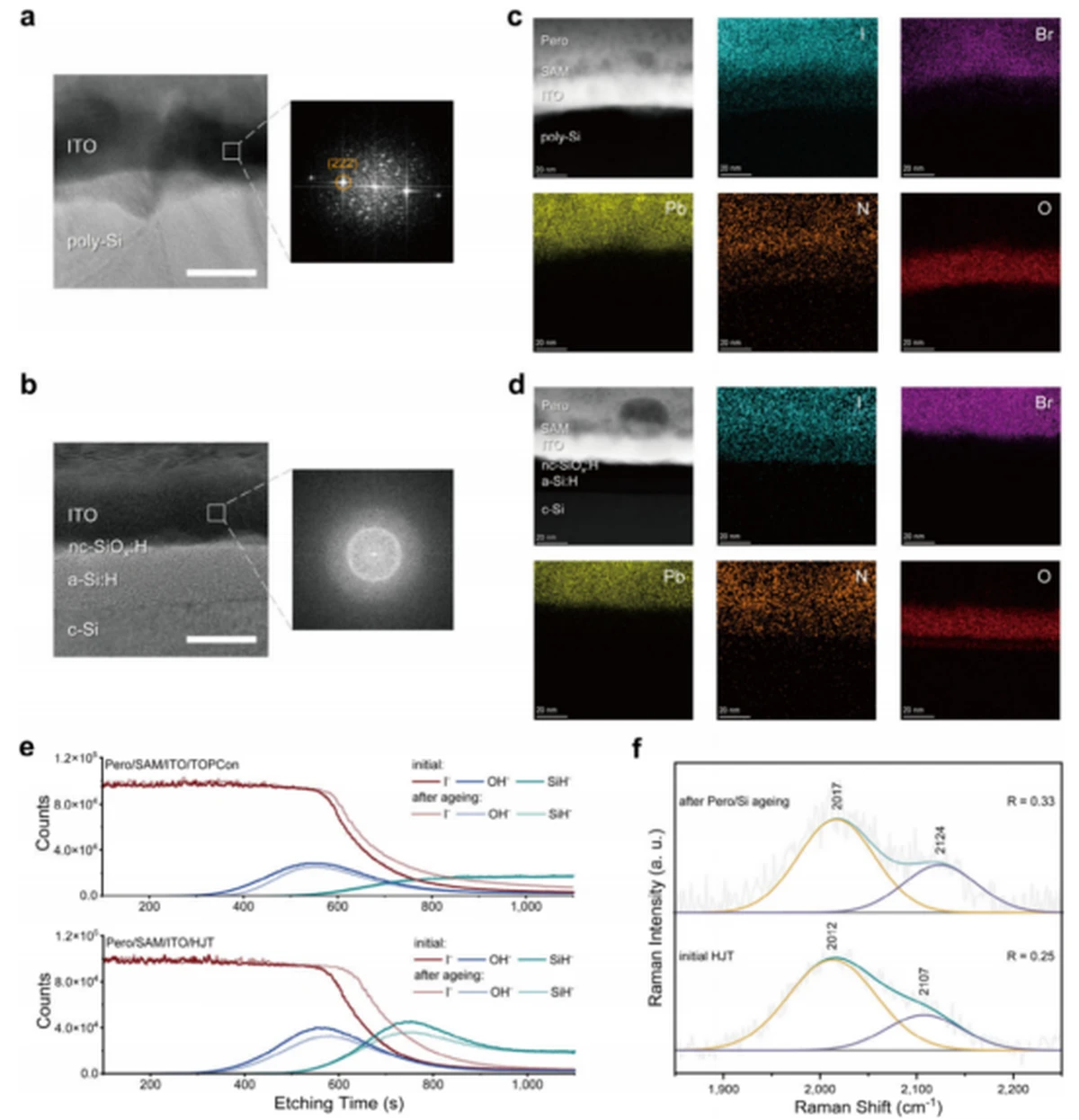
(a) TEM-FFT images of Pero/TOPCon and (b) Pero/HJT tandem interfaces (c) STEM-EDX elemental maps of Pero/TOPCon and (d) Pero/HJT interfaces after thermal aging (e) ToF-SIMS depth profiles of Pero/TOPCon and Pero/HJT interfaces before and after thermal aging (f) Near-surface Raman spectra of buried HJT silicon before and after thermal aging
Transmission electron microscopy and fast Fourier transform analysis revealed that ITO deposited on amorphous a-Si:H exhibited an amorphous structure, while ITO deposited on polycrystalline silicon was crystalline. Amorphous ITO possesses more pores and defects, providing pathways for ion and hydrogen migration. Elemental mapping (STEM-EDX) and time-of-flight secondary ion mass spectrometry (ToF-SIMS) confirmed that I⁻ and nitrogen-containing species penetrated more deeply into the HJT interface after aging. Raman spectroscopy further detected a reduction in Si-H bonds and increased structural disorder in HJT, indicating hydrogen out-diffusion from the a-Si:H layer and its participation in interfacial reactions.
This study provides mechanistic evidence for interface-driven interactions and degradation in perovskite/silicon tandem devices. The hydroxyl-rich amorphous ITO at the buried interface facilitates the migration of perovskite ions and silicon-hydrogen species, potentially accelerating cation deprotonation, PbI₂ formation, and silicon surface disordering in Pero/HJT structures. Consequently, the specific selection and processing of transparent conductive oxides likely modulate the reported ion/hydrogen migration pathways.
Therefore, future tandem designs aimed at suppressing interfacial interactions should consider: (a) employing dense TCOs with superior barrier properties (e.g., optimized ITO/IZO); and (b) exploring the introduction of additional ultrathin conformal barrier layers (e.g., ALD-grown oxides) to block ion/hydrogen transport. Understanding and addressing these factors is critical for achieving large-scale, long-lifetime applications of next-generation high-efficiency tandem photovoltaic devices.
Original Reference: Revealing the Interface Degradation of Monolithic Perovskite/Silicon Tandem Photovoltaics
contact
Be the first to know about our new product launches, latest blog posts and more. Nanjing Vision Potential Intelligent Technology Co.,Ltd.Established based on the Nanjing Xiangning Artificial Intelligence Research Institute, we have brought together a number of outstanding industry... Any question or request?
Click below, we’ll be happy to assist. contact