

- PV-Station-Solutions
- PV-Panel-Testing-Solutions
- Silicon-Ingot-Testing-Solutions

Raw Silicon Wafer SPL Inspection Equipment is a professional device for silicon wafer quality inspection based on the photoluminescence principle of silicon materials. It utilizes the intrinsic excitation luminescence properties of silicon: after excitation, electrons transition from the valence band to the conduction band, and then back to the valence band, emitting fluorescence. PL intensity is negatively correlated with defect density and recombination center concentration, so the quality of silicon wafers can be evaluated by detecting PL signals. Raw silicon wafer PL inspection technology can be widely applied in the early stages of photovoltaic product manufacturing processes such as ingots, raw wafers, textured wafers, enabling quality inspection during early process steps before and after cell diffusion, achieving the dual goals of product quality control and manufacturing cost savings.
 SC-SPL Device Diagram
Applied in key processes such as wafer sorters and texturing feeders for online or offline inspection of wafer quality, ensuring wafers entering subsequent processes meet standards.
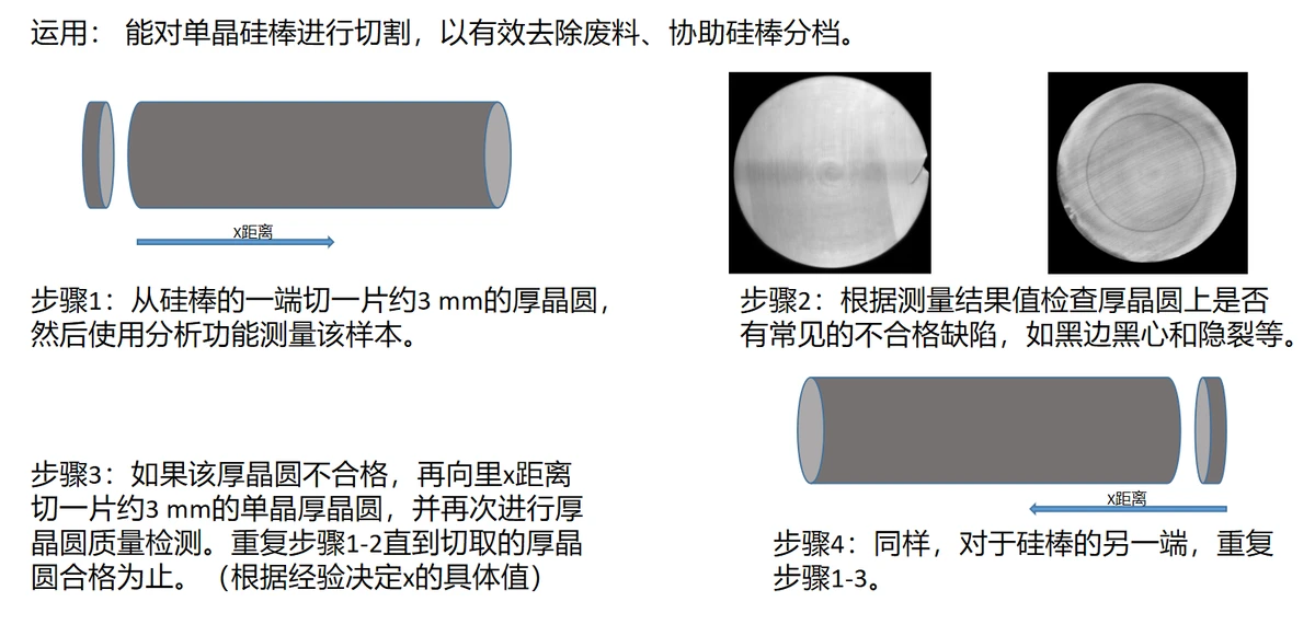
Cut and sample monocrystalline silicon ingots (approx. 3mm thick wafers), analyze thick silicon wafer quality, effectively remove waste material, and assist ingot grading. Detects defects like black edges, black cores, cracks.
Utilizing high-sensitivity PL, it inspects process wafers with low minority carrier lifetime, such as textured wafers, diffused wafers, etched wafers, identifying quality issues early in cell manufacturing and avoiding resource waste in subsequent steps.
Used in PV material and cell technology R&D to analyze intrinsic material properties and assess the impact of process parameters on wafer quality, serving as a core tool for performance analysis and process optimization.
Detects PL information of wafers and blocks before diffusion; compatible with monocrystalline, quasi-monocrystalline, and polycrystalline; detects defects like dislocations, filaments, grain boundaries; can be integrated into wafer sorters and texturing feeders.
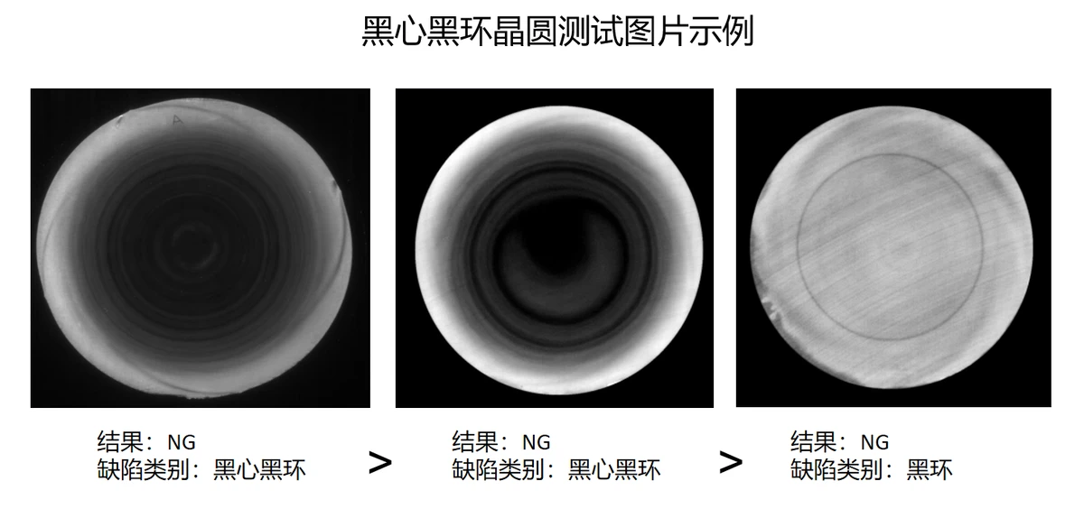
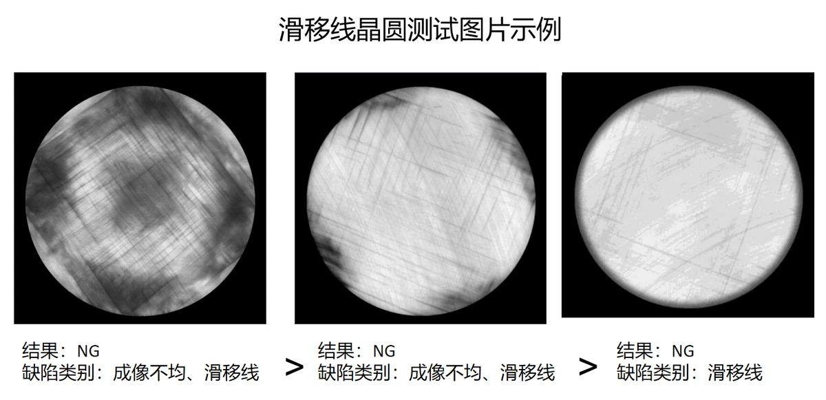
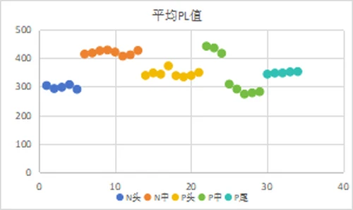
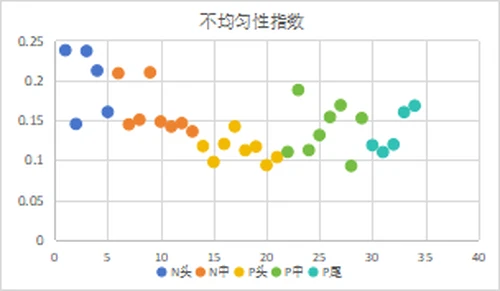
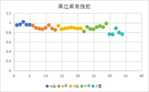
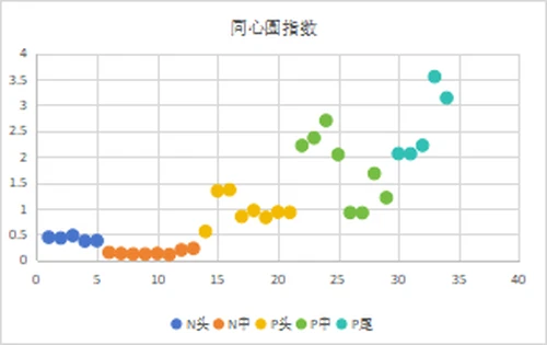
Identifies crystallographic defects not detectable by visual or crack inspection modules: blackening, dislocations, concentric circles, black corners, etc. Calculates PL value based on grayscale and defect area ratio; lower PL values indicate more severe defects.
Clearly detects concentric circle defects, accurately measures average PL grayscale. Can integrate with external production lines to output control signals for automated quality grading.
Analyzes approx. 3mm thick wafers cut from monocrystalline ingots, checking for defects like black edges, black cores, cracks. Iteratively cuts until qualified, effectively removing waste material and assisting ingot grading.
Utilizes the intrinsic excitation luminescence properties of silicon, requiring no electrical contact. PL intensity is negatively correlated with defect density and recombination center concentration, accurately reflecting the material's intrinsic quality.
Applicable for inspecting process wafers with low minority carrier lifetime, such as textured, diffused, and etched wafers, enabling early detection of quality issues in cell manufacturing and avoiding resource waste in subsequent processes.
Compatible with monocrystalline, quasi-monocrystalline, and polycrystalline wafers; inspects various forms including ingots, raw wafers, textured wafers; applicable for 156~210mm sizes (half/full wafers).
Detects dislocations, filaments, grain boundaries, cracks, blackening, black spots, black corners, black cores, black rings, concentric circles, etc. Can identify crystallographic defects not detectable by visual or crack inspection modules.
Calculates PL value based on grayscale and defect area ratio; provides multi-dimensional parameters such as black edge/black core index, non-uniformity index, concentric circle index; supports statistical analysis of sample test results.
| Parameter | Specification |
|---|---|
| Model | SC-SPL |
| Camera Specifications | NIR enhanced InGaAs camera, 1K line scan, exposure 10μs~10s, response 900-1700nm, max line rate 40kHz |
| Infrared Pixels | 1024×1 pixels |
| Lens Specifications | HD wide-angle 16/25/45mm optional, FOV ≥80°, telephoto lens optional |
| Light Source Specifications | Semiconductor laser, main wavelength 980±5nm |
| Spot Uniformity | ≥90% (within effective detection area) |
| Exposure Cycle | 20μs~100000μs, step 1ms adjustable |
| Detection Wavelength Range | 900~1300nm |
| Compatible Sizes | 156×156mm ~ 210×210mm (half/full wafers) |
| Inspection Objects | Ingot slices, crystalline silicon cell raw materials (crystal pulling, slicing, raw wafers, texturing) |
| Detectable Defect Types | Dislocations, filaments, grain boundaries, twin crystals, blackening, concentric circles, black corners, etc. |
| Stage Size | Adaptable to automated tracks (customizable) |
| Control Method | Proprietary host software fully automated control |
| Detection Accuracy | Crack width > 50μm detectable |
| Imaging Accuracy | ≥0.2mm/pixel |
| Focus Mode / Distance | Manual focus / 400-650mm |
| Hardware Mount | Aluminum profile, sheet metal, etc. |
| Inspection Time | 0.5s~2s (based on automation cycle) |
| Test Platform | Windows + standard AI inspection software |
| Power | 500-1000W |
| Power Supply Protection | Reverse current/overload/leakage/ESD/overheat protection |
| Computing Device | Industrial computer |
| Ambient Temperature | 15-50℃, Humidity 30%-70% (non-condensing) |
| Equipment Weight | Approx. 20kg (actual product prevails) |
| Dimensions | 400×350×800mm (L×W×H) |
| Power Supply | Single-phase AC220V±10%, 50HZ±1HZ |
| Defect Type | SPL Imaging | Imaging Analysis |
|---|---|---|
| Raw Silicon Wafer Concentric Circles | 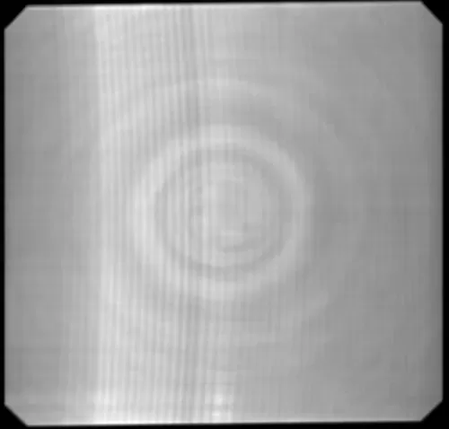 | This PL inspection of raw silicon wafers shows concentric circle defects, characterized by ring-shaped concentric textures. These defects are caused by uneven radial temperature gradient and pulling speed fluctuations during crystal growth, leading to periodic defect distribution along the radius. They disrupt subsequent process uniformity and reduce cell performance consistency, requiring optimization of radial parameters during crystal growth. |
| Grain Boundary | 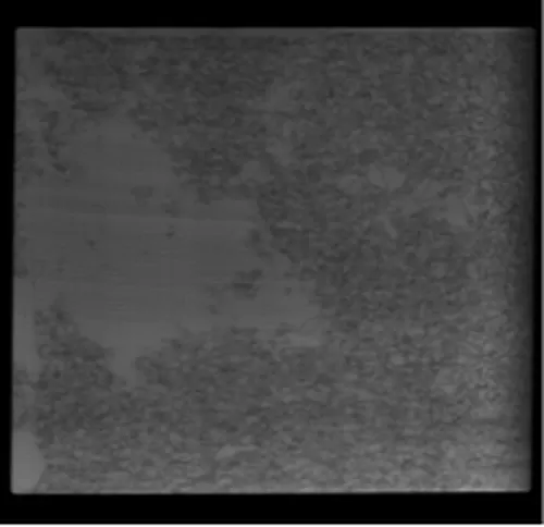 | This PL inspection of textured wafers shows grain boundary defects, appearing as mottled, mesh-like boundaries. Due to different grain orientations, the lattice arrangement at grain boundaries is discontinuous, causing uneven PL signals. Grain boundaries act as recombination centers, reducing carrier lifetime. This requires optimizing grain control during crystal growth or texturing process uniformity. |
| Concentric Circles | 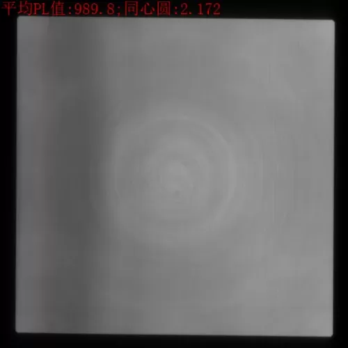 | This PL inspection of textured wafers (avg PL: 989.8; concentric circle index: 2.172) shows post-texturing concentric circle defects, characterized by ring-shaped concentric patterns. These defects arise from uneven chemical distribution and wafer rotation speed fluctuations during texturing, causing radial differences in etching depth. They impair texturing uniformity and affect subsequent process compatibility and carrier transport, requiring optimization of chemical distribution and rotation parameters. |
| Pre-Deposition Wafer | 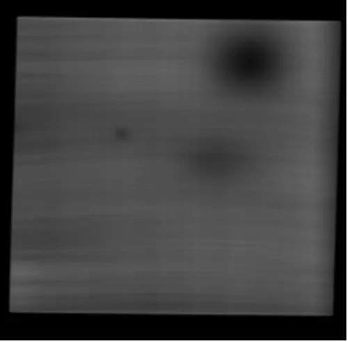 | This PL inspection of pre-deposition wafers shows block-shaped black spots and dot-like dark areas. These are caused by impurity aggregation in the raw substrate, surface contamination from previous processes, or physical damage. Such defects interfere with subsequent coating uniformity and hinder carrier transport, requiring improved cleaning and substrate quality control. |
| Black Core / Black Ring | 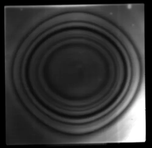 | This wafer SPL inspection shows black core/black ring defects, appearing as layered black bands (black ring) and ring-shaped brightness differences (black core). These are caused by uneven radial temperature fields and reaction gas distribution during diffusion, or by radial substrate defects manifesting after diffusion. They disrupt carrier distribution uniformity and reduce cell conversion efficiency, requiring optimization of radial parameter control in diffusion processes. |
| Scratches / Handling Marks | 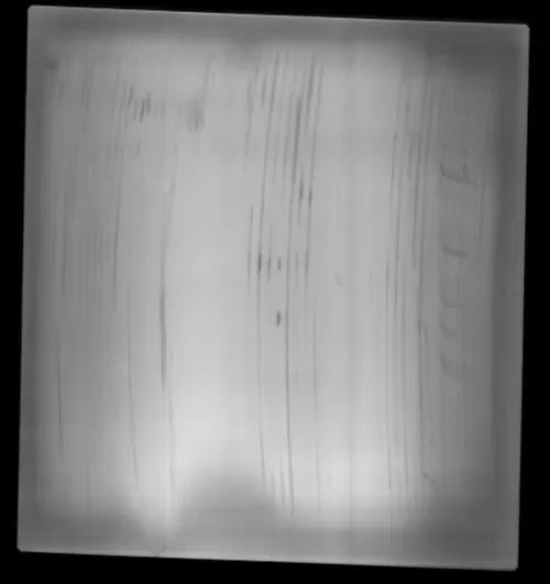 | This wafer SPL inspection shows scratches and handling marks: linear scratches and dot-like marks from physical contact or foreign objects during wafer handling and clamping. These defects interfere with diffusion uniformity and hinder carrier transport, requiring improved handling procedures and foreign object control. |
| Black Core / Black Ring (Wafer Slicing) | 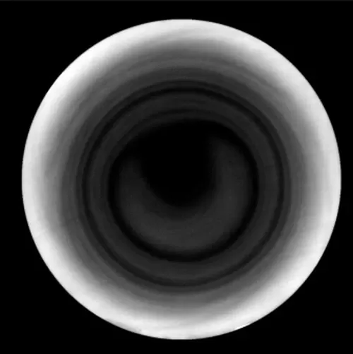 | This PL inspection of sliced wafers shows black core/black ring defects, characterized by dark center areas surrounded by ring-shaped black bands. These defects often result from impurity enrichment in the center during crystal growth, radial defect aggregation, or stress concentration during processing. They impair carrier distribution uniformity and cell stability, requiring targeted optimization of center region control during crystal growth and processing. |
| Ingot Concentric Circles | 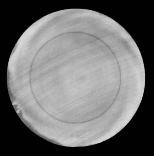 | This PL inspection of sliced wafers shows ingot concentric circle defects, appearing as characteristic ring-shaped patterns. These defects are caused by radial temperature gradient fluctuations during crystal growth or uneven radial stress during slicing, leading to periodic lattice misalignment. They affect cell performance consistency and require optimization of radial parameter control in related processes. |
| Stress Slip Lines | 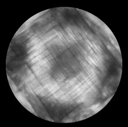 | This PL inspection of sliced ingots shows significant stress slip line defects, characterized by intersecting stripe patterns. These defects are caused by mechanical stress during slicing clamping and cutting, leading to atomic plane slip and lattice misalignment. They reduce carrier lifetime and affect subsequent cell conversion efficiency, requiring optimization of stress control parameters during slicing. |
The raw silicon wafer PL inspection equipment leverages the intrinsic luminescence properties of silicon to detect wafer defects early without electrical contact, controlling quality from the source and saving manufacturing costs. It can be widely applied in wafer production, ingot grading, process monitoring, and R&D fields, providing efficient and accurate inspection solutions for the photovoltaic industry.
检测出硅片中各种肉眼不可见缺陷
自动预测硅片的效率参考值
自动统计各缺陷与良品数量及比例,
产能大于6000片/小时
无接触式检测,不对硅片二次损伤
提前筛选出问题片,节约制造成本
contact
Be the first to know about our new product launches, latest blog posts and more. Nanjing Vision Potential Intelligent Technology Co.,Ltd.Established based on the Nanjing Xiangning Artificial Intelligence Research Institute, we have brought together a number of outstanding industry... Any question or request?
Click below, we’ll be happy to assist. contact