
- PV-Station-Solutions
- PV-Panel-Testing-Solutions
- Silicon-Ingot-Testing-Solutions
As the photovoltaic industry advances toward higher efficiency and greater diversity, crystalline silicon cells (PERC/TOPCon/HJT/xBC), perovskite single-junction cells, and crystalline silicon-perovskite tandem cells present new challenges for inspection technology. Traditional equipment typically supports either electroluminescence (EL) or photoluminescence (PL) imaging alone, making it difficult to perform cross-validation and comprehensive analysis on the same cell area.
Vision Potential has leveraged its deep expertise in optoelectronic inspection to independently develop the PLEL Integrated Machine SC-PLEL-PS. As the first domestic system integrating both EL and PL dual-mode luminescence imaging, this device enables synchronized comparative analysis on the same cell area, fully revealing defect morphology and distribution, and providing quantitative data support for photovoltaic technology iteration.
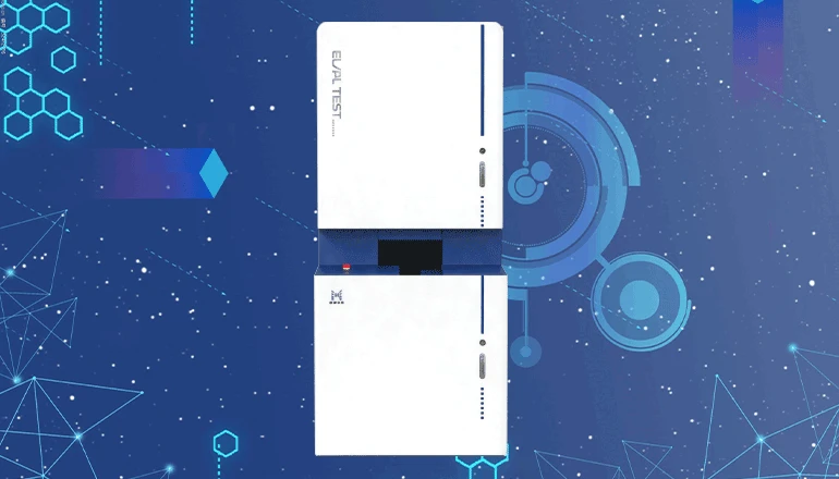
Vision Potential Crystalline Silicon/Perovskite PLEL Integrated Machine
Inperovskite PLinspection, the Vision Potential PLEL Integrated Machine features a highly stable semiconductor laser source (primary wavelength 808±5nm, with optional 450/915/980nm), spot uniformity ≥90%, and adjustable power from 0.1 to 2 suns. The laser excites the perovskite material to generate photoluminescence signals, captured by a high-sensitivity NIR camera (25 megapixels, response 400-1200nm).
PL image analysis enables precise evaluation of:
Film uniformity:Bright areas indicate good crystallization, while dark spots correspond to defect-rich regions or interfacial recombination centers
Defect density:Variations in luminescence intensity reflect non-radiative recombination losses
Composition segregation:Local luminescence anomalies suggest uneven perovskite composition
This capability is particularly valuable for process optimization during perovskite R&D and for incoming material inspection in production lines, eliminating defects at the source and reducing rework costs.
Forperovskite EL detection,the Vision Potential PLEL Integrated Machine is equipped with a high-precision programmable power supply (constant current/constant voltage dual mode, voltage 0-30V±1%, current 0-10A±1%). Electroluminescence is excited by current injection, and EL imaging clearly identifies:
Laser scribing deviations:Dark lines or broken regions indicate insufficient scribing precision
Micro-cracks and dark spots:Non-luminescent local areas suggest structural damage
Interfacial compatibility issues:In perovskite tandem cells, abnormal luminescence indicates carrier injection or extraction barriers
Electrode contact anomalies:Non-uniform grayscale reveals interface problems between electrodes and transport layers
The combination of EL and PL modes enables complementary analysis, with EL identifying current-blocking regions and PL detecting non-radiative recombination centers, fully revealing cell performance bottlenecks.
The Vision Potential PLEL Integrated Machine supports three major inspection categories:
Crystalline silicon cells:PERC、TOPCon、HJT、xBC
Perovskite single-junction and flexible cells
Crystalline silicon-perovskite tandem cells(bare/die-coated/encapsulated)
Whether for high-precision characterization in R&D laboratories or high-speed full inspection on production lines, the system offers flexible adaptability.
EL locks current-blocking regions caused by micro-cracks, while PL identifies non-radiative recombination centers at grain boundaries, fully revealing defect morphology and distribution.
Intelligent control of cylinders and motors enables automatic conveying, position calibration, and lifting, enhancing inspection efficiency and repeatability.
Standard 808±5nm, optional 450/915/980nm; spot uniformity ≥90%, power adjustable from 0.1 to 2 suns.
NIR-enhanced camera, maximum frame rate 4.5 FPS, imaging accuracy ≥0.1mm/pixel, capturing fine defects.
Proprietary algorithms analyze minority carrier diffusion length and lifetime (accuracy ±0.1μs for τ≤10μs), outputting IVoc, Jo, τ, and Rs Mapping.
Constant current/constant voltage dual mode, voltage 0-30V (±1%), current 0-10A (±1%), meeting various bias requirements.
The system includes proprietary PC software supporting:
Image processing: multiple adjustment modes and format saving
Data management: automatic report generation and traceability
Precise observation: cursor tracking and regional statistics
Intelligent analysis: automatic defect classification, MES integration
Mapping generation: IVoc, Jo, τ, Rs, etc.
Suns-Voc analysis: recombination behavior study
| Parameter | Specification |
|---|---|
| Model | SC-PLEL-PS |
| Camera | NIR-enhanced, 25 MP, response 400-1200nm, exposure 10μs~30s |
| Light Source | Semiconductor laser, 808±5nm (optional 450/915/980nm) |
| Spot Uniformity | ≥90% |
| Detection Accuracy | Crack width >50μm |
| Imaging Accuracy | ≥0.1mm/pixel |
| Inspection Time | 0.1s~10s (adaptive), ≤15s per cell |
| Defect Types Detectable | Micro-cracks, broken fingers, chips, scratches, cold solder, over-etching, dark spots, concentric rings, low-efficiency cells, contamination, etc. |
| Stage Size | 50×50mm ~ 230×230mm (customizable) |
| Dimensions | 1000×900×1600mm |
| Weight | Approx. 200kg |
The Vision Potential PLEL Integrated Machine has demonstrated excellent performance in:
Crystalline silicon PL:Evaluating crystallization quality and carrier lifetime
Perovskite PL:Analyzing film uniformity and defect density
Perovskite tandem PL:Focusing on perovskite layer characteristics and interface matching
Crystalline silicon EL:Identifying electrode contact anomalies, micro-cracks, and broken fingers
Perovskite EL:Detecting laser scribing deviations, micro-cracks, and dark spots
Perovskite tandem EL:Assessing interfacial compatibility and current matching
University research: defect mechanism studies, material characterization
Corporate R&D: next-generation high-efficiency cell development
Production line quality control: process fluctuation monitoring, parameter adjustment
Finished product grading: comprehensive defect screening, downstream risk mitigation
TheVision Potential PLEL Integrated Machine,with its core advantages of dual-mode imaging, quantitative analysis, and full-scenario coverage, provides a complete lifecycle inspection solution for crystalline silicon, perovskite, and tandem cells—from raw materials to finished products, and from R&D to mass production. In key applications such as perovskite PLandperovskite EL detection,the system delivers exceptional imaging quality and analytical capability, serving as a critical technological enabler for the photovoltaic industry’s pursuit of higher efficiency and reliability.
contact
Be the first to know about our new product launches, latest blog posts and more. Nanjing Vision Potential Intelligent Technology Co.,Ltd.Established based on the Nanjing Xiangning Artificial Intelligence Research Institute, we have brought together a number of outstanding industry... Any question or request?
Click below, we’ll be happy to assist. contact